PCB-Design is the skill to take your projects from breadboard to production. You can make your projects more permanent and durable, and share your designs with others! Additionally, PCB-Design Skills are sought after in the job market, whether you are doing hardware design specifically or just need to create a quick circuit for testing purposes.
With that being said, let’s start out on our PCB-Design Journey using the best Open-source design tool out there — KiCad! The first step will be downloading KiCad from their website here
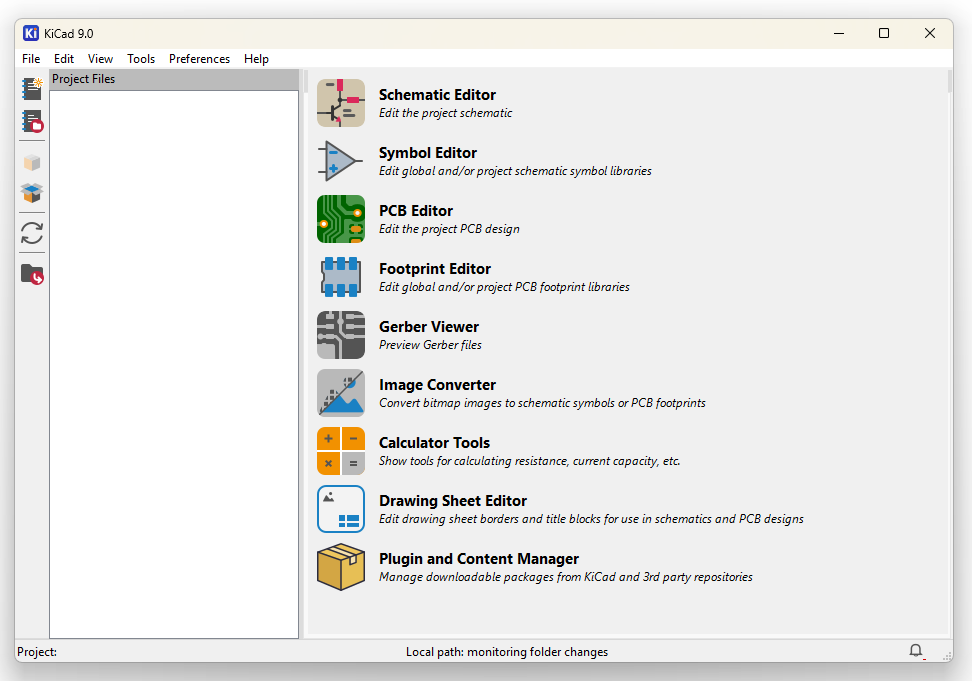
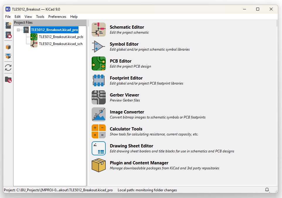
Once KiCad is installed, you are greeted with the window shown here:
The main applications we will be using are the Schematic- and Symbol-, as well as the PCB- and Footprint- Editor. They are grouped this way, because PCB Design happens in two domains: Schematic and Layout. Before continuing with the tutorial, I want to introduce a bit of theory about these two realms and how they are used in PCB design.
Schematic
The schematic holds information on the connections between individual Parts. It has nothing to do with the physical appearance, structure or dimensions of the part you are working with or their arrangement.
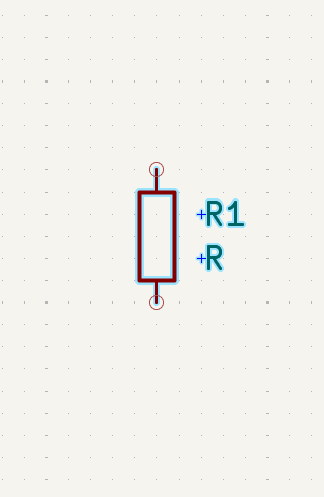
The defining building blocks here are called Symbols.
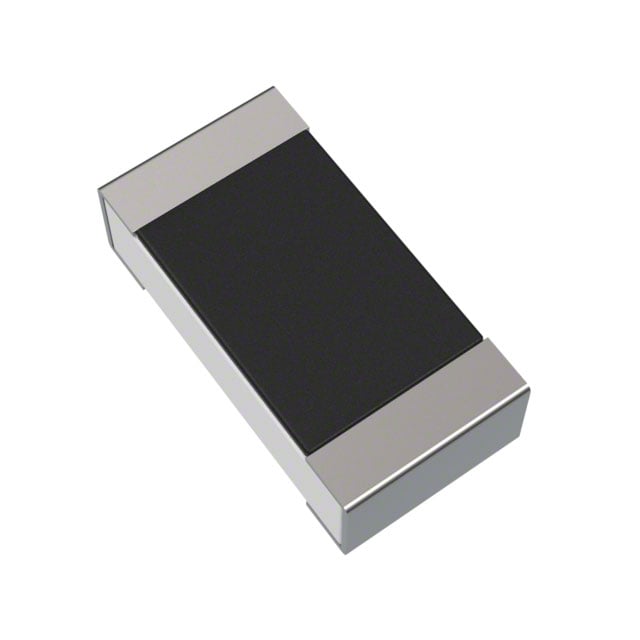
Take for example the simple resistors shown below. They are definitely physically different, but they share the same schematic symbol (shown on the right). All resistors that have 2 terminals can share the same Schematic Symbol, even if one is a meter in length and the other could be displaced by a light breeze. Most of the time in our workflow, we define the schematic first before moving on to the Layout.
When starting from a breadboard circuit, start by transferring all the components and connections from your breadboard into a schematic.

Layout
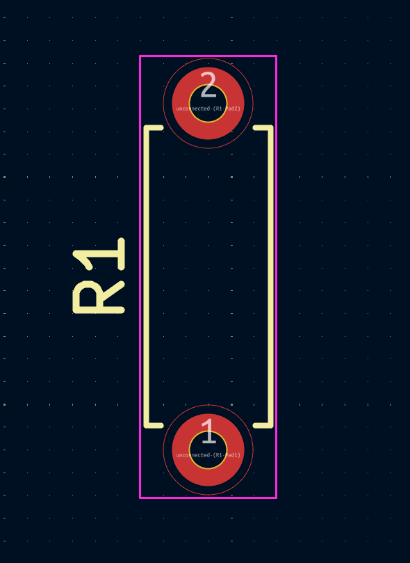
In the layout domain, we then reconnect with reality and take care of the physical arrangement of our components given their physical dimensions. The defining building blocks here are called Footprints. A Footprint like the ones shown below defines the device dimensions, labeling and connections. The connections can either take the form of exposed metal pads on the PCB Surface for surface mount devices (SMD) or holes through the PCB for through hole technology components (THT).

It is our job as PCB designers to arrange the components and layout the connections between them. To aid this task, KiCad shows thin lines between component pads according to the connections defined in the schematic.
The first project
For this example project we will design a simple breakout board for the TLE5012B E1000 angle sensor by Infineon because it is suitably easy and a real world application for an ongoing project of mine. To start a new project, we click the new Project Button in the top left corner of the KiCad window (![]() ). Find a suitable location for your projects files and give it a fitting name. I will name my project “TLE5012_Breakout”. Afterwards your project will be created with a Schematic and PCB file. Double-click the Schematic file and wait for the editor to open.
). Find a suitable location for your projects files and give it a fitting name. I will name my project “TLE5012_Breakout”. Afterwards your project will be created with a Schematic and PCB file. Double-click the Schematic file and wait for the editor to open.
Project-Schematic
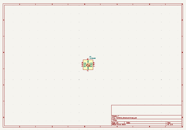
Inside the editor, we are greeted with an empty schematic, to which we will now add the TLE5012B IC by clicking the Place Symbol Button (![]() ) in the Right Symbol Tray. In the Choose Symbol Window, type “TLE5012” into the search bar and select the part from the list before clicking OK. Drag the Symbol to the middle and place it with a single left-click.
) in the Right Symbol Tray. In the Choose Symbol Window, type “TLE5012” into the search bar and select the part from the list before clicking OK. Drag the Symbol to the middle and place it with a single left-click.
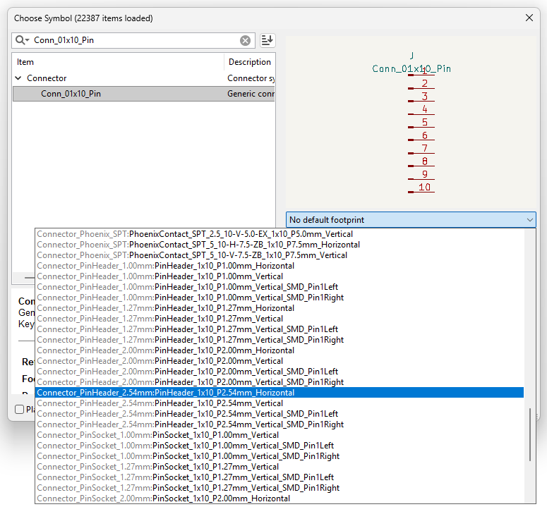
Your schematic should now look like the one shown on the left here. You will notice the Place Symbol Button icon is still attached to the cursor. Click inside the schematic again to now add the connector we want to use. I want to use a 10 Pin connector (Symbol Name: Conn_01x10_Pin). Since there are a multitude of connectors featuring 10 pins in a single row, we additionally need to specify which physical part we want to use. We can do this by using the dropdown on the right of the Choose Symbol Window and selecting the Connector_PinHeader_2.54mm:PinHeader_1x10_P2.54mm_Horizontal footprint like shown on the right below. After clicking OK, we can go ahead and place the Connector on the left edge of the schematic. The remaining components to be placed are three resistors (Symbol Name: R) and two capacitors (Symbol Name: C). The procedure is the same as for the connector. For the resistors, we will use the Resistor_SMD:R_0201_0603Metric_Pad0.64×0.40mm_HandSolder footprint and for the capacitors the Capacitor_SMD:C_0201_0603Metric_Pad0.64×0.40mm_HandSolder footprint.
Tip: To place multiple equivalent parts, just place one and copy it using Ctrl+C and Ctrl+V
Tip: If you want to stop using the place symbol tool, press Esc
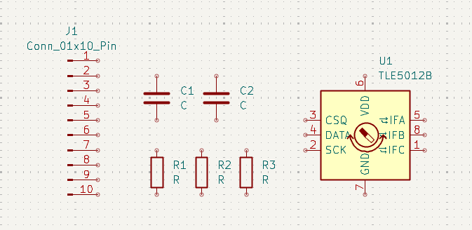
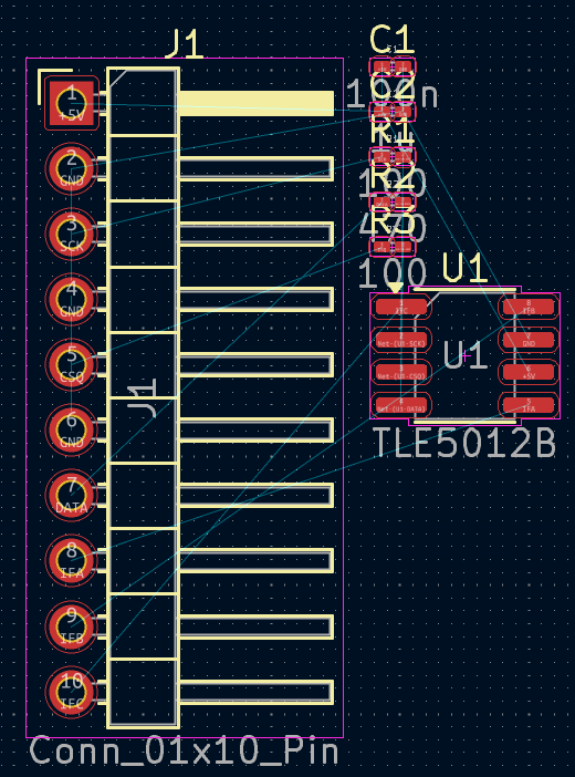
Having placed all symbols, the schematic looks something like the one below.
The fact that we need these components for the chip to work is taken straight from the TLE5012Bs datasheet (page 10, figure 5) in addition to a second decoupling capacitor because we will have long cable connections to the breakout board.
So the next step is connecting the components according to the datasheet. This is done using the Draw Wires tool (![]() ). Additionally, we can use the +5V and GND nets from the Place Power Symbol tool (
). Additionally, we can use the +5V and GND nets from the Place Power Symbol tool (![]() ) to manage the signal chaos a bit. The power symbols establish a connection between all nets they are connected to, making power routing a lot more elegant.
) to manage the signal chaos a bit. The power symbols establish a connection between all nets they are connected to, making power routing a lot more elegant.
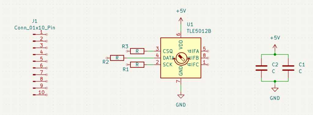
Using these tools I tried to rearrange the components a bit, connect them and move the labels around a bit to clean up the design. But connecting the Connector would still be a mess when simply running the signals around the ICs Symbol. To solve this issue, we can use the Place Net Labels tool.
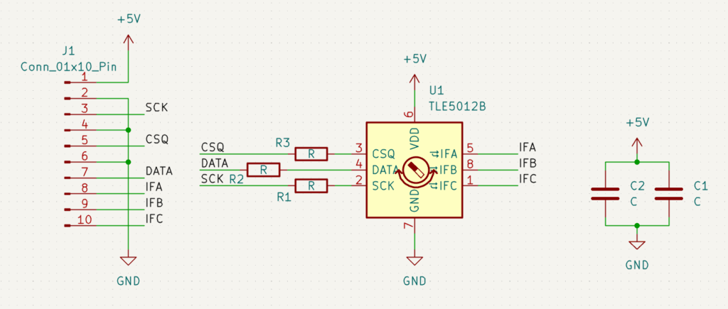
Extend a bit of signal line from the IC and Resistor pins, and then name each line using the Place Net Labels tool. You can then use the same technique to connect these nets to the pin-connector. Afterwards the schematic looks like this:
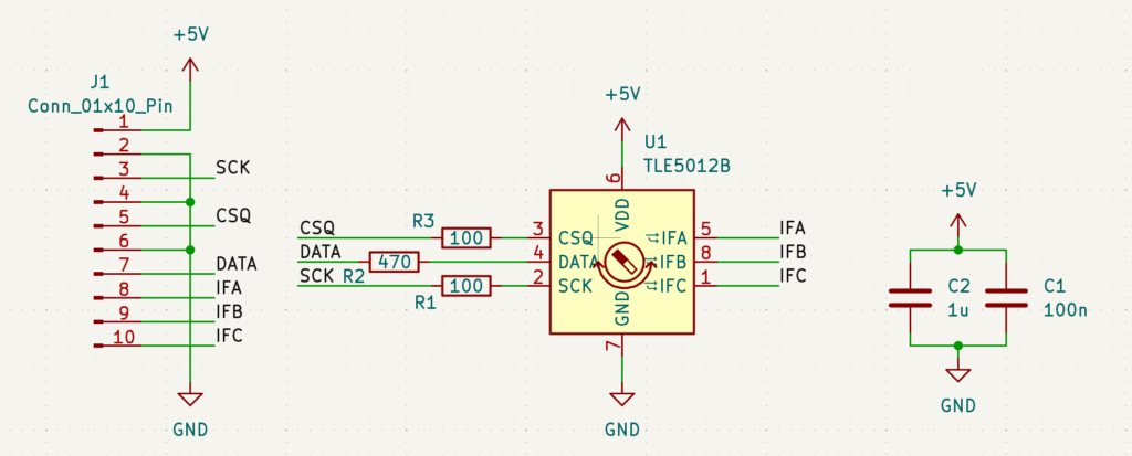
Now that everything is connected, the schematic is almost done. The last thing we need to do is assign values to the resistors and capacitors. Since they are standard components, they share the same symbol and footprint, even when they have different values. So to add these values, we double-click the component and enter the right values in the Value field. The finished schematic now looks like this:
Project-Layout
Now that the schematic is done, we can move on to the layout. Save the schematic using Ctrl+S and click the Switch to PCB Editor Button (![]() ) in the top-bar. The PCB Editor will also be initially blank. Each time, we want the PCB Editor to reflect the current state of the schematic, we need to use the Update PCB from Schematic button (
) in the top-bar. The PCB Editor will also be initially blank. Each time, we want the PCB Editor to reflect the current state of the schematic, we need to use the Update PCB from Schematic button (![]() ). In the upcoming window, click the Update PCB and then the Close button. You can now place the components somewhere in the center.
). In the upcoming window, click the Update PCB and then the Close button. You can now place the components somewhere in the center.
This is the way it looked for me. Notice the light blue thin lines. These indicate where connections need to be established. Before we start establishing the connections, we first design the board layout. Select the Edge.Cuts layer on the right and then the Draw Circles tool to create a 30mm radius circle. To place the sensor exactly in the board middle, we can set the Grid Origin to the circle center using the Grid Origin tool (![]() ). Then we can drag the TLE5012 to the center of the circle. It should snap into place.
). Then we can drag the TLE5012 to the center of the circle. It should snap into place.
We could also set the device coordinates to (0,0) although this is currently not working in my KiCad Version (9.0.4).
You can now drag around the components, rotating them using “R” or flipping them from one board side to the other using “F”.
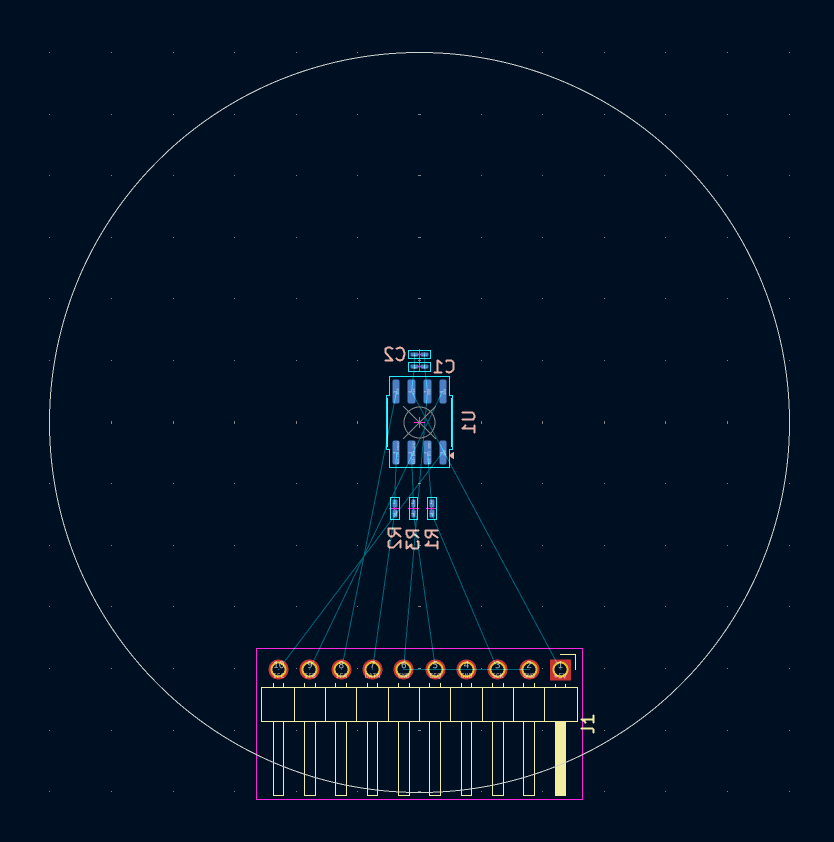
A simple component arrangement looks like this. Notice how most components have blue pads indicating that they are located on the back of the PCB. This way most connections are parallel, and we have reduced the number of vias we will need, which is always good in PCB design. In the next step, we use the Route Single Track tool (![]() ) to make all connections. We can select a track width by starting a track and then using the right-click menu, selecting Track/Via width, Use custom values … , and entering
) to make all connections. We can select a track width by starting a track and then using the right-click menu, selecting Track/Via width, Use custom values … , and entering 0.4mm for the track width. For some of the connections, you might need to use a via to resolve a trace crossing. Vias are connections through the PCB that connect the different layers with each other. To use a via, start the routing and then use the right-click dropdown and click on Place Through Via.
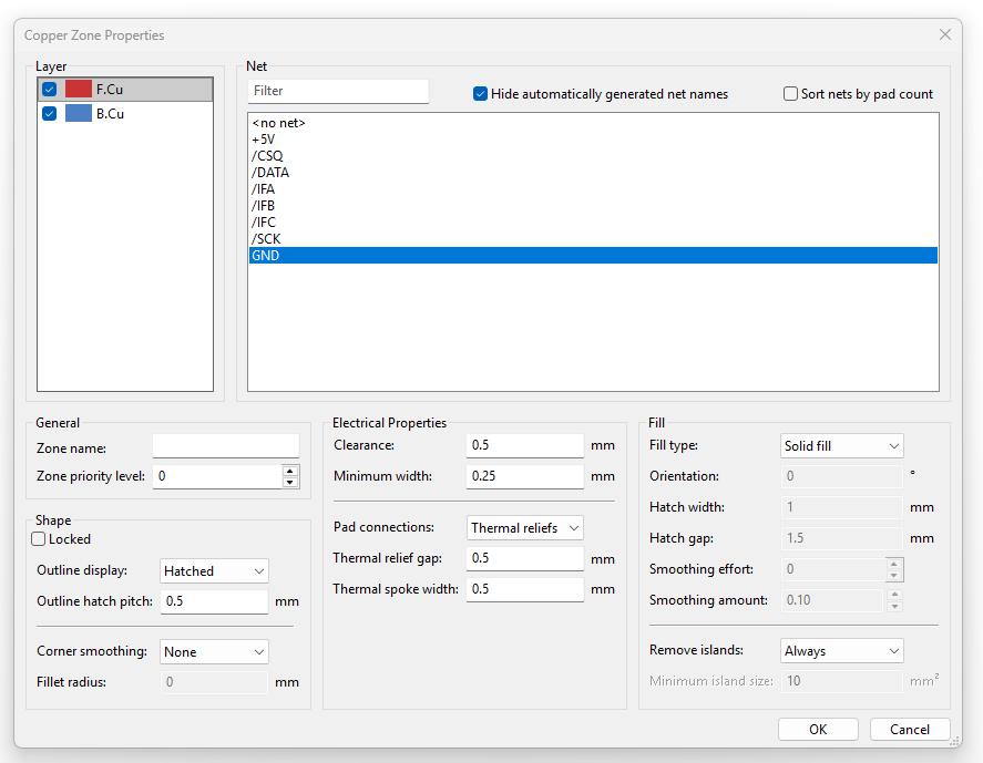
For improved signal integrity, we can add a ground plane. Just click the Draw Filled Zones button (![]() ). Click outside the PCB circle to start the polygon. In the upcoming dialogue, select both layers and the GND net with all other settings untouched and click OK. Draw a polygon around the PCB circle and click “B” once you are done to fill the layers.
). Click outside the PCB circle to start the polygon. In the upcoming dialogue, select both layers and the GND net with all other settings untouched and click OK. Draw a polygon around the PCB circle and click “B” once you are done to fill the layers.
And that’s it! You just designed your first PCB!
You can now add mounting holes to the design using the circle tool on the Edge.Cuts layer, or view your design in the 3D Viewer (![]() ). If you want to get your design produced, I can recommend JLCPCB or Digikey-Red depending on your needs. Both offer tutorials on how to export your design for their production service.
). If you want to get your design produced, I can recommend JLCPCB or Digikey-Red depending on your needs. Both offer tutorials on how to export your design for their production service.
If you want to broaden your PCB design knowledge, there are a ton of really great additional KiCad courses out there and the community is awesome. Also, most questions you might have can often times be easily solved with a quick Google search.